
Researchers develop perovskite X-ray detectors: A promising advance for lower-dose medical imaging
Researchers from the Shanghai Institute of Optics and Fine Mechanics (SIOM) at the Chinese Academy of Sciences, collaborating with colleagues from Central China Normal University, have developed a novel perovskite-based X-ray detector integrated with a complementary metal-oxide-semiconductor (CMOS) pixel array.
Their findings, published in the journal Nature Communications, demonstrate the potential of this technology to significantly enhance the performance of X-ray imaging systems used in medical diagnostics and treatment.
X-ray imaging plays a vital role in the diagnosis and management of cardiovascular diseases, cancers, and various other medical conditions. Direct-conversion X-ray detectors, which utilize semiconductor materials to directly convert X-ray photons into electrical signals, offer superior spatial and temporal resolution compared to traditional indirect-conversion detectors that rely on scintillator materials. However, the semiconductor materials currently employed, such as silicon (Si), amorphous selenium (a-Se), and cadmium-based compounds like CdZnTe and CdTe, have limitations in terms of X-ray absorption efficiency or high production costs, hindering their widespread adoption for general X-ray imaging applications.
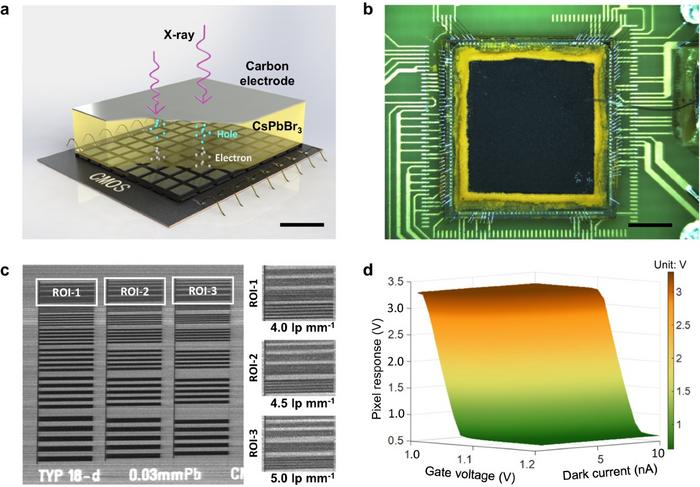
Inorganic CsPbBr3 based direct-conversion X-ray CMOS detector. (Image by SIAT)
Integrating perovskite films
Perovskite materials have emerged as a promising alternative to conventional semiconductors due to their favourable properties. However, the feasibility of integrating perovskite films with high-speed pixelated CMOS arrays, a critical component for advanced X-ray detectors, remained unexplored until now.
In this study, the researchers successfully developed a direct-conversion X-ray detector by screen-printing a 300-micrometer-thick inorganic cesium lead bromide (CsPbBr3) perovskite film directly onto a dedicated CMOS pixel array. Through rigorous characterization and testing, they demonstrated that the thick CsPbBr3 film exhibits a high mobility-lifetime product (μτ) of 5.2×10⁻⁴ cm2 V–1, a remarkable X-ray detection sensitivity of 15891 μC Gyair–1 cm–2, and a low dose detection limit of 321 nGyair s–1.
Superior performance of perovskite CMOS detector
Experimental X-ray two-dimensional (2D) imaging results showcased the superior performance of the perovskite CMOS detector, achieving a very high spatial resolution of 5.0 line pairs per millimeter (lp mm-1) with a hardware limit of 6.0 lp mm-1, while operating at an impressively low dose of 260 nGy. Furthermore, the researchers successfully validated the detector’s capability for three-dimensional (3D) computed tomography (CT) imaging at a rapid signal readout speed of 300 frames per second (fps).
“Our work shows the potential of lead halide perovskites in revolutionizing the development of state-of-the-art X-ray detectors with significantly enhanced spatial resolution, readout speed, and low-dose detection efficiency,” said Prof. GE, a lead researcher on the project. “This paves the road for medical X-ray imaging applications to become gentler and safer in the future.”
This breakthrough in perovskite-based X-ray detector technology holds promise for the development of next-generation medical imaging systems that can deliver higher-quality images while minimizing radiation exposure to patients. With further research and development, these detectors may enable safer and more accurate diagnostic procedures, ultimately improving patient care and outcomes across various medical specialties.
